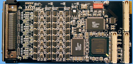
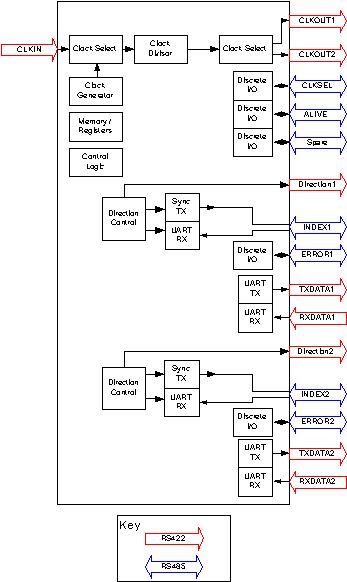
PMC-BiSerial II-NG1
PMC Compatible Bi-Directional Serial Data Interface


Please note that the PMC-BiSerial-II has been upgraded and the PMC-BiSerial-III is currently recommended for new designs

The PMC BiSerial-II NG1 is part of the PMC Module family of modular I/O components by Dynamic Engineering. The PMC BiSerial-II is capable of providing multiple serial protocols. The NG1 protocol implemented provides two full-duplex RS-422 UART interfaces with error detection, two half-duplex RS-485 custom index interfaces, external clock input, two clock outputs, and various discrete signal inputs and outputs, all using RS-485 transceivers.

The transmit data rate is derived from the 31.25 MHz on-board oscillator or external reference clock. The 31.25 MHz clock is divided by 2, 3, 4, 5, 6, 7, or 8 to generate the external clock outputs as well as the Tx clock for the UART and index interfaces.

The receive side of these interfaces uses a doubled (62.5 MHz) clock to sample the input data stream. The receiver uses the clock divisor to determine how many clock periods constitute a received bit period.

The FIFOs always operate at the PCI clock frequency of 33 MHz to simplify testing and operational functions.

Thirty-two differential I/O are provided for the serial signals. The drivers and receivers conform to the RS-485 specification (exceeds RS-422 specification). The RS-485 input signals are selectively terminated with 100Ω (82Ω resistor plus internal switch resistance). The termination resistors are in two-element packages to allow flexible termination options for custom formats and protocols. Optional pullup/pulldown resistor packs can also be installed to provide a logic 1 on undriven lines. The terminations and transceivers are programmable through the Xilinx device to provide the proper mix of outputs and inputs and terminations needed for a specific protocol implementation.

All configuration registers support read and write operations for maximum software convenience, and all addresses are long word aligned.

The PMC BiSerial-II conforms to the PMC and CMC draft standards. This guarantees compatibility with multiple PMC Carrier boards. Because the PMC may be mounted on different form factors, while maintaining plug and software compatibility, system prototyping may be done on one PMC Carrier board, with final system implementation on a different one.

The PMC BiSerial-II uses a 10 mm inter-board spacing for the front panel, standoffs, and PMC connectors. The 10 mm height is the standard height and will work in most systems with most carriers. If your carrier has non-standard connectors [height] to mate with the PMC BiSerial-II, please let us know. We may be able to do a special build with a different height connector to compensate.

The UART channels are each supported by a 32K by 32-bit FIFO. The FIFOs support long word reads and writes with a full 32-bit loop-back path for FIFO testing. Data is latched and the bus immediately released on a write-cycle. As soon as data is present in the FIFO it is pre-read to be immediately available for a read cycle. This allows minimal delay on the PCI write or read to/from the FIFO, as well as immediate access for the Tx and Rx state machines.

A 2048 by 8-bit internal FIFO is also provided for each UART channel to store response data. This FIFO can only be written to by the Rx state machine when receiving an acknowledge packet after a read or write packet has been sent. The response data is read over the PCI bus by the user software.

The index channels send a 9-bit data word when it is loaded into their data register, if enabled to do so. An immediate response of 9 or 12 bits is expected, which is stored in an internal register. The data available flag is set, which can be enabled to cause an interrupt, and the received data can be read over the PCI bus. Each channel has a separate direction output, which indicates whether the channel is currently functioning in transmit or receive mode.

The index channels can also send data from one or both of two pre-programmed data registers every 10 msec. If both registers are enabled the data word alternates between the two values. A12-bit loop count is provided to determine the number of words sent. If the loop count is zero the process will continue indefinitely.

An external clock input is available to receive an external 31.25 MHz clock reference. This input can also be used to receive a 1x data clock at the desired transfer frequency.

Two separately enabled clock outputs send the programmed transmit clock off the board for use by external circuitry.

There are five other bi-directional discrete I/O lines, two Error signals (Error1 and Error2), an Alive signal, a Clock Select signal, and a Spare signal. The direction and value of these signals is programmable with configuration register bits, when set to be an output, and read as a status bit, when set to be an input.

Various interrupts are supported by the PMC BiSerial-II NG1. An interrupt can be configured to occur when either FIFO becomes almost full or almost empty, when either response FIFO goes above _ full or below _ full, when index data is available or an index framing error is detected, or when either UART channel or either index channel times-out.

Further information including timing diagrams, register bit maps and descriptions, connector pinouts etc. are included in the hardware description manual. The Driver is described in the software reference manual. Please download the manuals for your reference.

PMC-BiSerial II-NG1 NG1 Block Diagram


If your situation demands a custom application then we will update the Xilinx FPGA. Send us your timing and we will send you the interface.... email us your wish list or call today!


Engineering Kits

PMC-BIS-II-NG1 ENG-1
Engineering Kit for PMC-BiSerial-II-NG1 includes: Board level Schematics [PDF], Software [Windows® 2000 Driver and reference application], HDEterm68-MP, HDEcabl68

PMC-BIS-II--NG1 ENG-2
Engineering Kit for PMC-BiSerial II-NG1 includes: PCI2PMC adapter card, board level Schematics [PDF], Software [Windows® 2000 Driver and reference application], HDEterm68-M, HDEcabl68


Related Products:

HDEcabl68 SCSI II/III Cable
HDEterm68 SCSI II/III to 68 pin terminal block
PCI2PMC PCI to PMC adapter card
PCIBPMC bridged PCI to PMC adapter card
cPCI2PMC cPCI to PMC adapter card 3U 4HP
PMC Extendio II PMC extension cable set - move your PMC up to 12" away from the host.


You must have Adobe Acrobat to read our PDF files.
PMC-BiSerial-II manual PDF
PMC-BiSerial-NG1 user manual PDF
NG1 Driver manual PDF


Custom, IP, PMC, PC*MIP, PCI, VME Hardware, Software designed to your requirements


Home | News | Search the Dynamic Engineering Site


[an error occurred while processing this directive]