Made in USA
The Embedded Solutions Experts
PCI-LVDS-8T
LVDS Transmitter card with 8 Channels of output
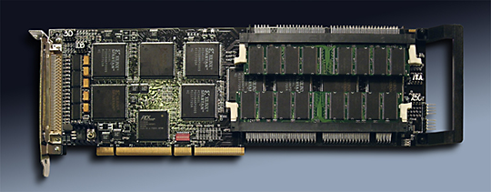

PCI-LVDS-8T Description
- 8 channels TIA/EIA-644 LVDS standard output.
- 2x4 channel configurations
- 2x256 MB SDRAM storage
- Scatter - gather DMA
- Independent clocking on output channels.
- Independent FIFO storage per channel.
- Flexible direct, transmit, and store modes of operation.
- Programmable output data filter.
- Programmable external clock input.
- Programmable external trigger input
- Universal PCI voltage interface
- Default configuration is to draw board power from the 3.3V power rails.
- 5V configuration is available - on board regulator to convert from 5V to 3.3V
- 1 year warranty standard. Extended warranty available.
- Extended [Industrial] Temperature standard.
- ROHS and Standard processing available
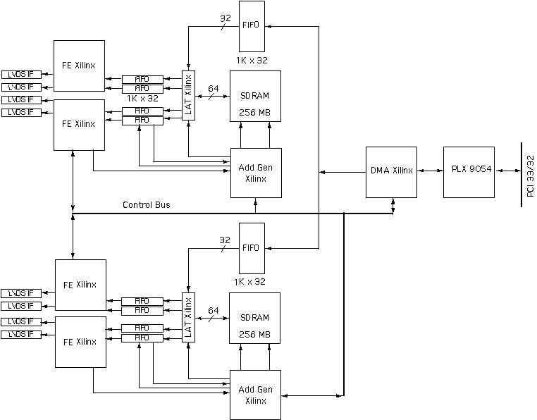
PCI-LVDS-8T is a PCI card with 8 channels. Each channel has memory, processing, and LVDS serialized output. The output is compatible with the TIA/EIA-644 LVDS standard. The serialized bit stream is transmitted with parallel serial data streams plus a reference clock. With the LVDS electrical standard long distances and quiet operation at high rates are possible. The TI interface device accepts a parallel word, and reference clock and outputs the seralized LVDS signals. The parallel word can be up to 21 bits. Each group of 7 bits are serialized independently using the common reference clock and upconverted to the LVDS transmit clock at 7X the parallel rate. The base model "8T" uses 14 of the 21 bits for the data and control. The "2T" model uses all 21 bits of the parallel interface.
The 8 channels are programmable with the ability to enable the channels of interest, the size of the memory allocated to each channel, the method of transmission and the synchronization of each transmission. Each channel is supported with independent FIFO memory at strategic locations to allow full speed operation and the use of the banked SDRAM.
The data to be transmitted is loaded into the SDRAM using DMA transfers. Once the memory is loaded the hardware is programmed for type of transmission. Looping with repeated data, single pass, and combinations are possible. For example a preamble can be sent once, then loop through the body of data a programmable number of times, and then a post amble can be sent. Standard single pass data can also be sent. The SDRAM is in two blocks. Each block is assocated with 4 channels. The start address for each channel can be programmed as well as the length of the data to be sent allowing all of the memory to be allocated to once channel or one quarter to each channel or whatever is required. For example in the "2T" model all of the memory for each bank is allocated to a single channel in each bank. In standard "8T" operation the channels are set-up in a symmetrical fashion.
Data is read from the memory and loaded into the FIFO associated with that channel. The Latch Xlinx converts from 64 bit SDRAM data down to 32 bit FIFO and upconverts the reference rate to keep the pipeline balanced. Data is moved in Bursts whenever there is enough to move a complete page. Any LW coherent size can be moved with the hardware automatically making the necessary paging adjustments.
Once in the FIFO the transmission section can read the data and format for moving to the Serializers. In the case of the "8T" the data width is reduced, and tags inserted to control the flow. In the "2T" the processing is different as all 21 bits of the serializers are used. The upper bits are used for flow control within the "2T" and stripped off prior to transmission. The final stage is preloaded when the channels are enabled locally.
If programmed to use an external trigger the hardware will then wait for that trigger event before starting to send the programmed sequence of data. External clocks and triggers can be used and the "8T" design supports retransmission of the clock and trigger to allow multiple boards to be controlled in a daisy chain fashion. The clock and trigger are accepted at the front panel and retransmitted at the rear to allow for internal chassis wiring. When the external trigger is not used the channels can still be started coherently via software with the master strart bit.
The first customers for the 8R and 8T needed to use multiple cards within each chassis. Specifically 10 cards were placed into an expansion chassis providing 80 channels. The power consumption is not particularly high, and with 10 cards was too much for the 5V or the 3.3V rail of the power supply. The cards come with an option to operate using the 5V or the 3.3V power rail as the main source of power to allow multple boards to be used in the same chassis without overloading the power supply - it is recommended that you mix 5V and 3.3V cards when working with multiple cards. Please note that the PCI interface is "universal voltage", and not affected by the power rail option.
For more complete information please download the hardware manuals. Bit maps, diagrams, pinouts etc. are contained within.
PCI-LVDS-8T Block Diagram
PCI-LVDS-8T Features Under Construction
Size
Full length PCI card.
PMC Compatible Slots
2 PMC slots provided.
Clocks
PCI primary bus can operate at 133, 100, 66, or 33 MHz. Secondary side can operate at the same or lower frequency compared to the primary side
Access Width
Standard PCI byte lanes supported for byte, word, and long-access dependent on installed PMC. 64- or 32-bit operation from either bus supported by Bridge.
Access Frequency
Bridge supports 133, 100, 66, or 33 MHz operation.
Software Interface
Industry Standard 31154 Bridge register definitions. The bridge does not require any user set-up. PMC register definitions as defined by installed hardware.
Interrupts
INTA, INTB, INTC, INTD, routed to PCI connector from both PMC slots. Most PMCs use one interrupt level [INTA]. User switches allow independent mapping of the PMC interrupt request to the PCI connector. Slot 0 is usually mapped to INTA and slot 1 to INTB. In addition, the interrupts can be routed [controlled] with DIP Switch between the PMC positions to support local PrPMC control.
Power
+5V, +12V, -12V regulated or PCI +3V supplied to PMCs.
VIO
Primary side set by PCI bus. Secondary side set by user selection [shunt]. Regulated 3.3V or 5V via MOSFET to VIO mini-plane.
Thermal
The PCIBPMCX2 has cut-outs to support increased airflow over the PMC component side. Optional fan(s) with 4 mounting positions are available.
IO Interface
Front bezel IO supported at PCI bracket. Jn4 user IO supported with either SCSI or DIN connectors. See Panduit for mate [120-964-455] or standard SCSI II connector. Optional support for Ethernet and Serial ports from PrPMC devices.
Specification
PCI, PCI-X, PICMG 2.15 specification compliant
LEDs
+3V, +5V, +12V, -12V, and Busmode 1 [present] for each slot plus VIO.
DIP Switch
4-8 position switches are provided to allow for configuration control and to select the primary and secondary clocking options.
JTAG
Primary PCI JTAG connections are made to the Bridge. The PMC JTAG connections are tied to labeled headers. One header following the Altera standard and one compatible with Xilinx and other manufacturers.
PCI-LVDS-8T Benefits Under Construction
Speed
PCIBPMCX2 offers PCI-X and PCI speeds plus a second PMC slot for designs with more than one PMC. For local processing, the rear slot can be used for a PrPMC with the IO or signal processing in the front slot. The Host computer can set-up operation, and then the PrPMC can use the local bus for high speed data transfer with the second PMC.
Price
PCIBPMCX2 is competitively priced. Make use of existing PMC designs in PCI applications without paying for the expense of a new design and layout. Save PCI slots with two PMCs in one location. Quantity discounts are available.
Ease of Use
PCIBPMCX2 is easy to use. A plug-and-play interface to the PMC site. The Bridge can be configured with the user switches on board, which eliminates the requirement for special software for the bridge itself. The PCIBPMCX2 has a bridge with Transparent and Non-Transparent modes. Standard drivers for the PMCs can be used without any software required for the carrier. The board comes configured for a 66 MHz capable primary bus and 33 MHz secondary bus. In most cases, the switches can be left with the factory settings. The manual contains clear directions for switch options. The engineering kit provides a good starting point for a new user.
Availability
We work to keep PCIBPMCX2 in stock, but it is a popular product. Dynamic Engineering has in house manufacturing capabilities for short lead times on larger orders.
Size
The PCIBPMCX2 is a full-size PCI board, which conforms to the PCI mechanical and electrical specifications. Eliminate mechanical interference issues. The PCIBPMCX2 can be used in all full-length PCI compliant slots.
PMC Compatibility
PCIBPMCX2 is PMC compliant per the IEEE 1386 specification. All Dynamic Engineering PMC modules are compatible with the PCIBPMCX2. All other PMC modules, which are compliant with the PMC specification, are compatible with the PCIBPMCX2. PCI3IP can be expected to work in any PCI compliant backplane.
PCI Compatibility
PCIBPMCX2 is PCI compliant. The PCIBPMCX2 can be expected to work in any PCI compliant backplane. The PCIBPMCX2 has been tested in multiple backplanes.
Part Number: PCI-LVDS-8T
Ordering Options
- PCI-LVDS-8T Standard board Add any of the following build options after the PN as shown below:
- -3.3V 3.3V Power Rail Operation
- -5V 5V Power Rail Operation
- -ROHS Use ROHS processing. Standard processing is "leaded"
- -CC Option to add Conformal Coating
Breakout Kits - PCI-LVDS-8T-ENG Break Out Kit includes: Board level Schematics [PDF], LVDS Cable and Windows® XP/2000 software driver
PCI-LVDS-8T Drivers
Software Support for PCI-LVDS-8T is included in the Engineering Kit.
PCI-LVDS-8T Manuals
Click on the link to Download selected manuals in PDF format.
Download the PCI_LVDS_8T Manual updated 4/10/02 in PDF format.
Download the PCI_LVDS_2T Manual updated 6/4/07 in PDF format.
Download the PCI_LVDS_8T NT Driver Manual updated 4/11/02 in PDF format.
Download the PCI_LVDS_8R /8T Windows XP/2000 Driver Manual updated 4/20/04 in PDF format.
Download the PCI_LVDS_2R /2T Windows XP/2000 Driver Manual 07/14/06 in PDF format.