Made in USA
The Embedded Solutions Experts
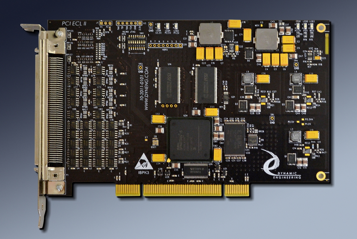
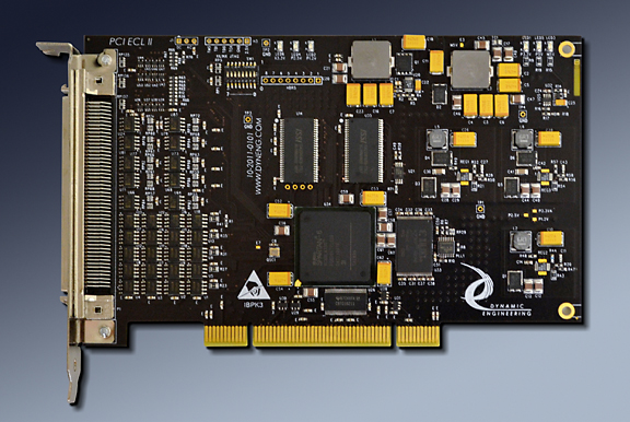
PCI-ECL-II
PCI-ECL-II - with Spartan 6 FPGA, 16Mx32 SDRAM, 20 ECL TX , 20 ECL RX, and 12 TTL IO
Order This Item
Contact sales@dyneng.com to order this item.Built to order using our on-site manufacturing capability.
PCI-ECL-II Description
- Industrial Temperature
- PCI 33/32 1/2 length card
- 20 transmit and 20 receive NECL/ LVPECL differential pairs
- Matched length, controlled impedance routing
- 12 TTL IO
- Local Power Supplies for ECL voltages
- SDRAM - 32 Mbytes x2
- Bezel IO and Rear IO for installed VPX device
- 1 Year Warranty Standard. Extended Warranty Available.
- ROHS and Standard Processing Available

Do you feel the need for speed? Differential ECL / NECL is still the interface of choice for high speed in noisy environments. PCI-ECL-II is an upgrade to the original PCI-ECL design. The IO connector pinout is maintained to allow ease of porting to the new platform. 20 ECL Inputs and 20 ECL Outputs plus 12 TTL IO are controlled via the FPGA. NECL, LVPECL and other ECL translators can be installed to meet IO requirements. The IO are matched length and impedance controlled. The Spartan VI FPGA provides the PCI interface, SDRAM interface, and IO interface with plenty of room for control, storage, filtering. and other control functions. With the SDRAM controller design, data can be stored for retransmission and looped if desired. The SDRAM can also be configured for FIFO like data handling. All options are selectable with software.
PCI-ECL-II features an integrated PCI interface with DMA support and ECL/TTL IO. The Spartan VI FPGA ties the PCI bus to the IO with storage and processing. Several models are offered and Dynamic Engineering can design a customized solution for you. See the partial list of available designs implemented on PCI-ECL and PCI-ECL-II. The Xilinx is reconfigurable, and supported with reprogrammable FLASH. Windows® and Linux SW solutions can be provided.
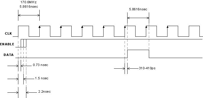
The ECL IO is routed to provide 100 ohm differential impedance, and matched length from the pin edge on the D100 connector to the Xilinx [BGA] Ball. All of the TX are matched, and all of the RX are matched to allow for high speed designs with tight timing requirements. Several ECL input bits are tied to clock capable input pins on the Xilinx to allow for external reference clocks.
The Xilinx is supported by a programmable PLL. The PLL is programmed with a serial bus via the Xilinx control register set. The driver handles this function. We recommend using the Cypress calculator to determine the PLL settings. The PLL supplies four clocks to the Xilinx which can be used for custom state-machine support.
In addition to the PLL, a client selected oscillator position is supplied. The default oscillator frequency is 50 MHz. and is used as the reference for the PLL. The oscillator frequency can be changed if required.
The ECL section has 20 inputs and 20 outputs. The state-machine can be programmed to use any number of the IO. The remaining IO can be used for a general purpose parallel port. Serial and Parallel interfaces can be implemented. For example, with a 4 wire serial interface a 16 bit parallel port will be available.
The SDRAM and internal Block RAM are used to store data from reception or for transmission. The memory is large enough that the IO can operate without interruption. The system can "go away" and not under or over-flow the memory. SDRAM is 32 MBytes in size per device. There are two devices on the board. Assuming a TX/RX channel on each SDRAM and allocating ½ of the memory to TX and to RX there are 16 MBytes per function. Further, assuming a continuous transmission is being supported, a 100 Mbit/sec serial data link, and DMA operation in use; the memory will support 1.34 seconds of system interruption. Similarly the Rx side can operate for 1.34 seconds before overflowing [assuming no handshaking in the design]. The memory can be allocated in software providing for asymmetrical operation, all on TX or all on RX for example.
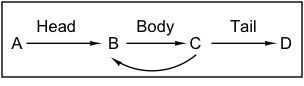
The SDRAM can also be configured to retransmit data. The memory can be partitioned into a header, body, and tail. The body can be repeated a programmable number of times. The header => body=>tail loop can then be repeated or stop at completion. All under software control. In continuous mode interrupts can be generated at the end of each major loop. The boundaries are programmable to allow for customized sizes.
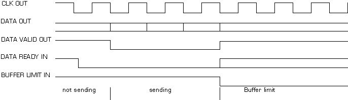
The Internal FIFO is to support DMA. The data is pipelined into or out of the FIFO under control of the scatter gather DMA engine. Data can also be moved with non DMA read or write operations. Data stored into the FIFO is moved to the main memory (SDRAM) and vice-versa. A state-machine moves the data with a burst transfer when there is sufficient data to move, and single transfers when near the boundary conditions. The state-machine for the data transfer operates autonomously. Each function has a separate DMA engine to allow for parallel TX and RX operation without software intervention.
Multi-board operation is supported. With multiple PCI-ECL-IIs in your system and unique cabling, sensors etc. for each slot it is important to "know" which PCI-ECL-II is which. A surface mount "dip switch" is provided to provide an identifier to the software. A specific PCI-ECL-II can be matched up with the PCI address allocated to make for deterministic control. The switch can also be used for other purposes; configuration control or debugging for example. The switch values are available to be read via the PCI bus.
The reprogrammable FLASH memory stores the Xilinx design file. The JTAG header is used to load the FLASH using the Xilinx standard IMPACT® software and download cable.
The IO is brought to a "D100" connector. The connector on PCI-ECL-II is a available in the standard right angle or a vertical mount. The right angle connector mounts through the bezel allowing for IO outside of the chassis. The vertical connector is used with a blank bezel and is optimized for internal to the chassis IO requirements. The mating connector is the AMP 5749621-9. Dynamic Engineering has cables and a break-out for this connector. HDEterm100 can be used to create a terminal block interface. HDEcabl100 is the standard cable. Customer specific cables can be manufactured. Please forward your connector and pin assignment requirements if you are interested in custom cables. In addition Dynamic Engineering has a "cross over" cable which can be used to interconnect two PCI-ECL-II cards or to connect to your equipment if you adopt the connector definitions that we used. The Pinouts are available within the manuals.
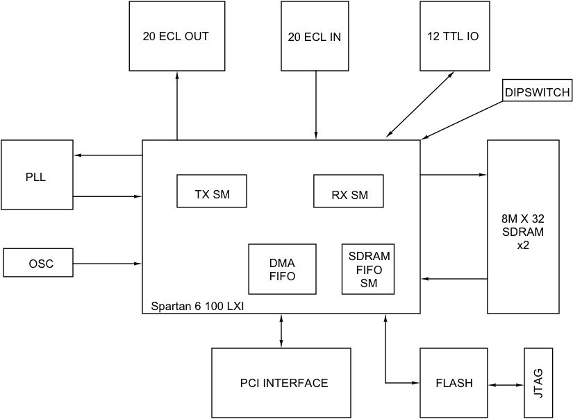
Block Diagram of PCI-ECL-II
PCI-ECL-II features an integrated PCI interface with DMA support and ECL/TTL IO. The Spartan VI FPGA ties the PCI bus to the IO with storage and processing. Several models are offered and Dynamic Engineering can design a customized solution for you. See the partial list of available designs implemented on PCI-ECL and PCI-ECL-II. The Xilinx is reconfigurable, and supported with reprogrammable FLASH. Windows® and Linux SW solutions can be provided.
The ECL IO is routed to provide 100 ohm differential impedance, and matched length from the pin edge on the D100 connector to the Xilinx [BGA] Ball. All of the TX are matched, and all of the RX are matched to allow for high speed designs with tight timing requirements. Several ECL input bits are tied to clock capable input pins on the Xilinx to allow for external reference clocks.
The Xilinx is supported by a programmable PLL. The PLL is programmed with a serial bus via the Xilinx control register set. The driver handles this function. We recommend using the Cypress calculator to determine the PLL settings. The PLL supplies four clocks to the Xilinx which can be used for custom state-machine support.
In addition to the PLL, a client selected oscillator position is supplied. The default oscillator frequency is 50 MHz. and is used as the reference for the PLL. The oscillator frequency can be changed if required.
The ECL section has 20 inputs and 20 outputs. The state-machine can be programmed to use any number of the IO. The remaining IO can be used for a general purpose parallel port. Serial and Parallel interfaces can be implemented. For example, with a 4 wire serial interface a 16 bit parallel port will be available.
The SDRAM and internal Block RAM are used to store data from reception or for transmission. The memory is large enough that the IO can operate without interruption. The system can "go away" and not under or over-flow the memory. SDRAM is 32 MBytes in size per device. There are two devices on the board. Assuming a TX/RX channel on each SDRAM and allocating ½ of the memory to TX and to RX there are 16 MBytes per function. Further, assuming a continuous transmission is being supported, a 100 Mbit/sec serial data link, and DMA operation in use; the memory will support 1.34 seconds of system interruption. Similarly the Rx side can operate for 1.34 seconds before overflowing [assuming no handshaking in the design]. The memory can be allocated in software providing for asymmetrical operation, all on TX or all on RX for example.
The SDRAM can also be configured to retransmit data. The memory can be partitioned into a header, body, and tail. The body can be repeated a programmable number of times. The header => body=>tail loop can then be repeated or stop at completion. All under software control. In continuous mode interrupts can be generated at the end of each major loop. The boundaries are programmable to allow for customized sizes.
The Internal FIFO is to support DMA. The data is pipelined into or out of the FIFO under control of the scatter gather DMA engine. Data can also be moved with non DMA read or write operations. Data stored into the FIFO is moved to the main memory (SDRAM) and vice-versa. A state-machine moves the data with a burst transfer when there is sufficient data to move, and single transfers when near the boundary conditions. The state-machine for the data transfer operates autonomously. Each function has a separate DMA engine to allow for parallel TX and RX operation without software intervention.
Multi-board operation is supported. With multiple PCI-ECL-IIs in your system and unique cabling, sensors etc. for each slot it is important to "know" which PCI-ECL-II is which. A surface mount "dip switch" is provided to provide an identifier to the software. A specific PCI-ECL-II can be matched up with the PCI address allocated to make for deterministic control. The switch can also be used for other purposes; configuration control or debugging for example. The switch values are available to be read via the PCI bus.
The reprogrammable FLASH memory stores the Xilinx design file. The JTAG header is used to load the FLASH using the Xilinx standard IMPACT® software and download cable.
The IO is brought to a "D100" connector. The connector on PCI-ECL-II is a available in the standard right angle or a vertical mount. The right angle connector mounts through the bezel allowing for IO outside of the chassis. The vertical connector is used with a blank bezel and is optimized for internal to the chassis IO requirements. The mating connector is the AMP 5749621-9. Dynamic Engineering has cables and a break-out for this connector. HDEterm100 can be used to create a terminal block interface. HDEcabl100 is the standard cable. Customer specific cables can be manufactured. Please forward your connector and pin assignment requirements if you are interested in custom cables. In addition Dynamic Engineering has a "cross over" cable which can be used to interconnect two PCI-ECL-II cards or to connect to your equipment if you adopt the connector definitions that we used. The Pinouts are available within the manuals.
Block Diagram of PCI-ECL-II
PCI-ECL-II Features
Size
½ size PCI card.
IO
20 ECL TX, 20 ECL RX, 12 TTL IO
Clocks
PLL [Cypress 22393], PCI, OSC, External clock sources are available for use
FPGA
Spartan 6 100 LX
PCI Bus
33 MHz 32 bit PCI bus implementation with DMA. Universal Voltage keying
Power
On board power supplies create +3.3, +2.5, +1.2, and -5V.
Interrupts
PCI interrupt scheme is supported
IO Interface
D100 connector. Pinout in manual. Right angle standard, Vertical mount available.
Specification
PCI specification compliant
LEDs
Voltage monitor circuits show operational voltages present
Humidity
PCI-ECL-II is a standard industrial grade board, able to handle 10-90% non-condensing humidity. If you need to have a board used in a more harsh environment, add -CC to add humi-seal after final test
JTAG
FPGA JTAG connections are tied to a labeled header. Add -JTAG to part number for this option to be installed.
Weight
Approximately 5 oz for non Humi-sealed board
Dipswitch
An 8 position switch is available to support multi-board operation or other user defined purposes
Statement of Volatility
Download the Statement of Volatility in PDF format.
PCI-ECL-II Benefits
Speed
PCI-ECL-II is designed for speed. The PCI bus is supported with DMA and an internal holding FIFO. The State-Machines interoperate with the SDRAM and support FIFOs [block RAM]. The NECL IO can operate up to 250 MHz. A separate state machine keeps the data flowing between the internal FIFOs and SDRAM. True pipelined operation can be implemented between the system memory and the external device.
Price
PCI-ECL-II combined with custom design is an attractive package
Ease of Use
PCI-ECL-II is easy to use. Windows® / Linux Drivers are available. Please download the manual(s) and see for yourself. Breakout and cable available.
Availability
PCI-ECL-II is built to order. Dynamic Engineering features co-located manufacturing and Engineering allowing for quick turn-around for off-the-shelf and custom IO projects
Size
PCI-ECL-II is a ½ size PCI board which conforms to the PCI mechanical and electrical specifications. Fits in the small form factor chassis as well as standard [full length]
PCI Compatibility
PCI-ECL-II is universal voltage PCI compliant device. PCI-ECL-II can be expected to work in any PCI compliant backplane.
Part Number: PCI-ECL-II
Ordering Options
- PCI-ECL-II Standard board - for a base version and standard processing
- -ROHS Use ROHS processing. Standard processing is ""leaded"
- -CC Option to add Conformal Coating
- -VC Switch to vertical connector with blank bezel to accomodate internal to chassis wiring. This option previously called -1.
- -JTAG Add installation of the JTAG header
- -MODEL Add suffix for a particular version [RTN10 etc]. See manuals tab for descriptions.
PCI-ECL-II Drivers
Software Support is available with [Linux / Windows] drivers for each model [see manuals page]. Each package has a combination of User Application and system files to support the user in developing their application. The reference SW package [User Application] is a great place to start development with examples of board use - loopback testing etc.
PLL Support
Download the CyberClocks R2.01.00 software
right click on the above link to download and save the cyberclocks zip folder to your target
PLL Support
Download the CyberClocks R2.01.00 software
right click on the above link to download and save the cyberclocks zip folder to your target
PCI-ECL-II Manuals
Models designed for or ported to -II PCB
Current Design
PCI-NECL-II-RTN10
Customer: Raytheon
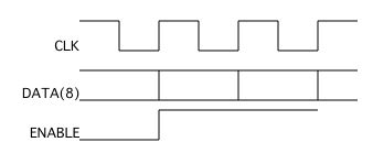
Custom Parallel interface. 8 bit parallel data path [NECL input and output] with reference clock and enable. Data valid on programmable edge of clock, enable active high. Programable use of enable. DMA support, 12 bits uncommitted TTL IO. Updated with higher performance memory operation, increased FIFO size, added status, and operational enhancements. Recommended for new designs Client tested with standard and external chassis.
Download the PCI-NECL-II-RTN10 Hardware Manual in PDF format.
Download the PCI-NECL-II-RTN10 Linux revision 1.0.5 Manual in PDF format .
Shown for reference
PCI-NECL-II-STE3
Customer: Singapore Technologies Electronics Limited
Custom Parallel interface. 8 bit parallel data path with reference clock and enable. Data valid on falling edge of clock, enable active high. DMA support, 12 bits uncommitted TTL IO. STE3A is recommended for new designs.
STE3 is available for previously integrated systems.
Download the PCI-NECL-II-STE3 Hardware revision A/B Manual in PDF format.
Download the PCI-NECL-II-STE3 Windows® revision A/B Manual in PDF format.
PCI-NECL-II-STE3A
Customer: Design Update
Custom Parallel interface. 8 bit parallel data path [NECL input and output]with reference clock and enable. Data valid on falling edge of clock, enable active high. DMA support, 12 bits uncommitted TTL IO. Updated with higher performance memory operation, increased FIFO size, added status, and operational enhancements. Client tested with standard and external chassis.
Download the PCI-NECL-II-STE3A Hardware revision A1 Manual in PDF format.
Download the PCI-NECL-II-STE3A Linux revision 1.0.3 Manual in PDF format .
Models implemented on orginal PCB; can be ported to -II PCB
Porting this model will include an update SW package
Download the PCI-NECL-XG1 Hardware revision A2 Manual in PDF format.
Download the PCI-NECL-XG1 XP/2000 Driver Manual in PDF format.
Porting this model will include an update SW package
Download the PCI-NECL-ASN1 Hardware revision B Manual in PDF format.
Download the PCI-NECL-ASN1 XP/2000 Driver Manual in PDF format.
STE1 has been ported and updated to STE3 and further updated to RTN10
Download the PCI-NECL-STE1 Hardware revision B Manual in PDF format.
Download the PCI-NECL-STE1 XP/2000 Driver Manual in PDF format.
Current Design
PCI-NECL-II-RTN10
Customer: Raytheon
Custom Parallel interface. 8 bit parallel data path [NECL input and output] with reference clock and enable. Data valid on programmable edge of clock, enable active high. Programable use of enable. DMA support, 12 bits uncommitted TTL IO. Updated with higher performance memory operation, increased FIFO size, added status, and operational enhancements. Recommended for new designs Client tested with standard and external chassis.
Download the PCI-NECL-II-RTN10 Hardware Manual in PDF format.
Download the PCI-NECL-II-RTN10 Linux revision 1.0.5 Manual in PDF format .
Shown for reference
PCI-NECL-II-STE3
Customer: Singapore Technologies Electronics Limited
Custom Parallel interface. 8 bit parallel data path with reference clock and enable. Data valid on falling edge of clock, enable active high. DMA support, 12 bits uncommitted TTL IO. STE3A is recommended for new designs.
STE3 is available for previously integrated systems.
Download the PCI-NECL-II-STE3 Hardware revision A/B Manual in PDF format.
Download the PCI-NECL-II-STE3 Windows® revision A/B Manual in PDF format.
PCI-NECL-II-STE3A
Customer: Design Update
Custom Parallel interface. 8 bit parallel data path [NECL input and output]with reference clock and enable. Data valid on falling edge of clock, enable active high. DMA support, 12 bits uncommitted TTL IO. Updated with higher performance memory operation, increased FIFO size, added status, and operational enhancements. Client tested with standard and external chassis.
Download the PCI-NECL-II-STE3A Hardware revision A1 Manual in PDF format.
Download the PCI-NECL-II-STE3A Linux revision 1.0.3 Manual in PDF format .
Models implemented on orginal PCB; can be ported to -II PCB
Porting this model will include an update SW package
Download the PCI-NECL-XG1 Hardware revision A2 Manual in PDF format.
Download the PCI-NECL-XG1 XP/2000 Driver Manual in PDF format.
Porting this model will include an update SW package
Download the PCI-NECL-ASN1 Hardware revision B Manual in PDF format.
Download the PCI-NECL-ASN1 XP/2000 Driver Manual in PDF format.
STE1 has been ported and updated to STE3 and further updated to RTN10
Download the PCI-NECL-STE1 Hardware revision B Manual in PDF format.
Download the PCI-NECL-STE1 XP/2000 Driver Manual in PDF format.